Platinum FET Test Chips, Optimized for 2D Materials
Title:
DefaultTitle
$85.38
$65.68
Please select combo product attributes
The combo subtotal is $,SAVE$
Product Details
+
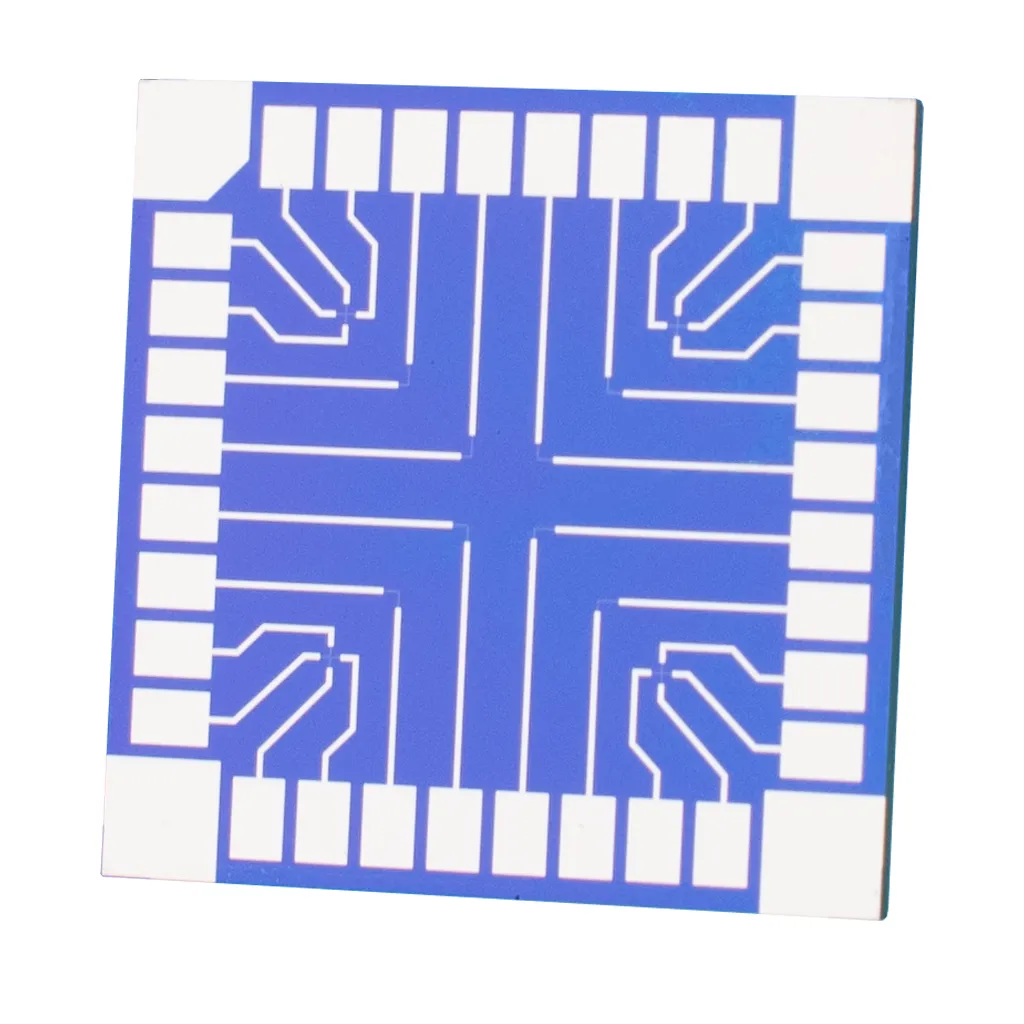
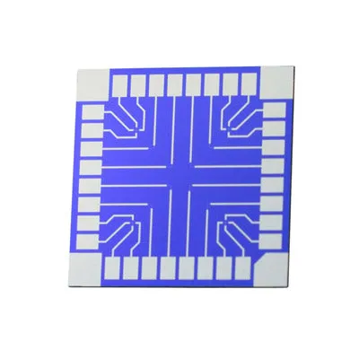
Ossila’s 2D material FET test chip is designed to allow users to perform electrical and optical measurements on monolayer or few-layer 2-dimensional (2D) crystals, without the need for expensive lithography equipment. Our chips come prepatterned with platinum electrodes on a Si-SiO2 substrate, with source-drain channel lengths ranging from 4 µm to 20 µm. Transfer your crystal across the channel and you are ready to measure. The chips also feature dual channel electrodes that allow you to stack two crystals on top of each other and contact each separately.
Research into 2D materials has been steadily growing in popularity for several years, fuelled by the promise of revolutionary new technology in areas ranging from batteries to quantum computers. The preferred method for 2D material preparation (within the research community at least) is the so-called 'Scotch-tape' method, where monolayer or few-layer crystals are peeled from bulk material. This method currently gives the highest quality 2D materials needed for optical and electronic applications. The preparation of 2D materials in this way is relatively straightforward, and optical measurements can require little more than a microscope and a light source.
However, to reach their full potential, the electrical characteristics of 2D materials needs to be studied. This posses a large barrier to entry for the researcher, as complicated and expensive lithography equipment is required to create the electrical contacts to the 2D crystals. We have developed our 2D material FET substrates in partnership with researchers in the field to remove this barrier, and to speed up the electrical and optical characterisation of 2D materials.
Electrode layout on 2D material FET material test chips (click to enlarge)
The platinum is sputtered onto a titanium adhesion layer to provide an extremely robust contact and channel allowing it to withstand cleaning procedures such as solvent sonication, plasma etching, and swabbing.
Surface topography of a dual-electrode pair
Electrical measurements on small 2D crystals can be tricky. It usually involves a multistage process consisting of:
Exfoliation of a bulk crystal into a 2d flakes
Locating a suitable flake
Transfer of the flake onto a substrate
Designing electrodes around the flake
Patterning of electrodes, usually using ebeam lithography
Metal deposition and lift-off
The Ossila test chips optimized for 2D materials help simplify this workflow by providing pre-patterned platinum electrodes onto which a flake can be directly transferred. This eliminates the need for access to lithography and deposition systems.
The electrode contacts are placed along the edges of the test chip, allowing optical measurements to be carried out without obstruction from wires.
Left: Depiction of a 2D flake spanning a variable gap channel. The position of the flake determines the channel width. Right: Two 2D flakes arranged on dual-pair electrodes
Cleaning
Your substrates may arrive with a residue from the photolithography process used to create the electrodes. We recommend cleaning the substrates before use by sonication in warm isopropanol for 10 minutes, followed by drying with compressed nitrogen. The substrates may be cleaned and reused as needed.
Electrode pair before (left) and after (right) sonication in warm isopropanol for 5 minutes (click to enlarge)
Sample preparation
Our guide to 2D exfoliation will walk you through the process preparing a suitable crystal for transfer, and deterministically positioning a flake on a substrate.
Electrical connections
The 32 rectangular pads are source-drain contacts. Once a flake has been positioned across the channel, the pads connected to electrodes on each side of the channel should be identified and a voltage applied across them. There are 3 different electrode geometries on the chip:
Dual electrodes in an inline configuration with fixed channel width (4 µm and 10 µm)
Quad electrodes in cross configuration with fixed channel widths (4 µm x 10 µm, 4 µm x 20 µm, 10 µm x 20 µm and 10 µm x 40 µm)
Dual electrodes in a perpendicular configuration which allows the channel width to be defined by the size of the crystal
Microscope images of some of the electrodes on the 2D material test chip (click to enlarge)
A probe station can be used to connect to the pads. Alternatively, a wire can be attached using conductive silver paint.
A wire attached to an electrode pad with conductive silver paint
The gate can be contacted directly through the substrate bottom or edges, or the 4 corner pads can act as the gate contact. If using the corner pads, we recommend applying silver (conductive) paint along and around the pad edges to make a connection with the substrate edge.
Conductive silver paint applied to connect a gate pad to the substrate edge
Over time a native oxide layer of a few nanometers thickness will build up on the exposed silicon. Removing this will allow a lower resistance electrical connection to the gate. If required, we recommend removing the native oxide mechanically by using a fine grit sandpaper or scratching the silicon area before making the contact. We do not recommend chemical removal of the native oxide as this process may damage the platinum electrodes and gate dielectric.


 - Fisherman Sandal Lightweight")


